🛠🛠🛠 𝐓𝐫𝐢𝐩𝐩𝐥𝐞 𝟐𝟎-𝐛𝐢𝐭 𝐃𝐀𝐂 𝐛𝐨𝐚𝐫𝐝 𝐦𝐚𝐧𝐮𝐟𝐚𝐜𝐭𝐮𝐫𝐢𝐧
Manual solder paste application, component placement, and reflow soldering form the backbone of my DIY electronics assembly.
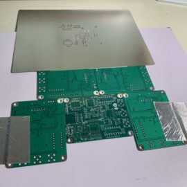
1️⃣ The process starts with the 𝗺𝗮𝗻𝘂𝗮𝗹 𝗮𝗽𝗽𝗹𝗶𝗰𝗮𝘁𝗶𝗼𝗻 𝗼𝗳 𝘀𝗼𝗹𝗱𝗲𝗿 𝗽𝗮𝘀𝘁𝗲. With the aid of a stencil that matches your PCB layout, solder paste is spread across the board, depositing a small amount on each pad where a component will sit. This task requires a steady hand and a keen eye to ensure the paste is applied evenly without smearing or bridging between pads.
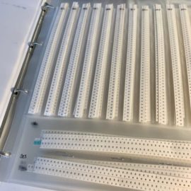
2️⃣ After solder paste application comes the intricate job of 𝗰𝗼𝗺𝗽𝗼𝗻𝗲𝗻𝘁 𝗽𝗹𝗮𝗰𝗲𝗺𝗲𝗻𝘁. Using a pair of tweezers, each component is carefully placed onto the corresponding solder-pasted pad on the PCB. This stage demands a lot of precision and patience, as components can be extremely small and need to be oriented correctly.
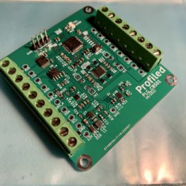
3️⃣ Finally, the board is ready for 𝗿𝗲𝗳𝗹𝗼𝘄 𝘀𝗼𝗹𝗱𝗲𝗿𝗶𝗻𝗴. The PCB, with all its delicately placed components, is put into a reflow oven. The oven heats the board following a specific temperature profile to melt the solder paste and create a solid electrical and mechanical connection between the components and the board. After a cooling period, the board comes out with all components firmly and neatly soldered in place.
This process, while demanding care and attention to detail, can be incredibly satisfying as you see your design come to life. It allows you to have a hands-on approach to hardware development, and fosters a deep understanding of the assembly process, which can be invaluable in designing for manufacturability in the future.


