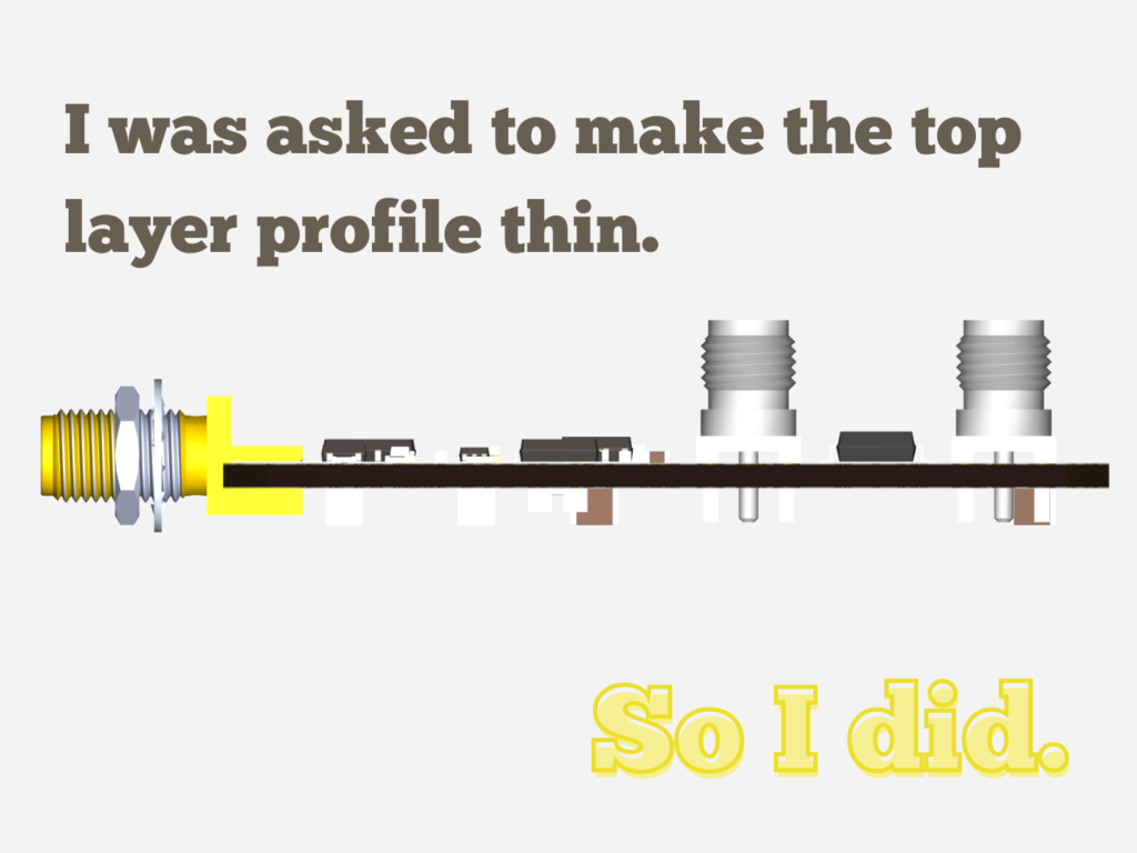
📄📄📄 𝐀 𝐭𝐡𝐢𝐧 𝐜𝐨𝐦𝐩𝐨𝐧𝐞𝐧𝐭 𝐩𝐫𝐨𝐟𝐢𝐥𝐞 𝐏𝐂𝐁 𝐥𝐚𝐲𝐨𝐮𝐭
Recently, I was tasked with designing a 𝗡𝗼𝗶𝘀𝗲 𝗔𝗺𝗽𝗹𝗶𝗳𝗶𝗲𝗿 where the top layer component profile had to be as thin as possible. It’s not just about choosing low-profile components, but also considering their placement, thermal management, and ensuring the integrity of the design.
Designing with such constraints requires a fair bit of creativity. I had to meticulously arrange components, rethink routing strategies, and consult passive components datasheets, definitely more than usual.
The result? A 𝗡𝗼𝗶𝘀𝗲 𝗔𝗺𝗽𝗹𝗶𝗳𝗶𝗲𝗿 board with thin top layer profile. It’s moments like these that remind me why I love diving into the intricacies of PCB design. Every constraint is an opportunity to innovate!
Thin component layout


